- 您现在的位置:买卖IC网 > Sheet目录3890 > PIC16C765T-I/L (Microchip Technology)IC MCU OTP 8KX14 USB 44PLCC
PIC16C745/765
DS41124C-page 94
Preliminary
2000 Microchip Technology Inc.
The following steps should be followed for doing an A/D
conversion:
1.
Configure the A/D module:
Configure analog pins / voltage reference /
and digital I/O (ADCON1)
Select A/D input channel (ADCON0)
Select A/D conversion clock (ADCON0)
Turn on A/D module (ADCON0)
2.
Configure A/D interrupt (if desired):
Clear ADIF bit
Set ADIE bit
Set GIE bit
3.
Wait the required acquisition time.
4.
Start conversion:
Set GO/DONE bit (ADCON0)
5.
Wait for A/D conversion to complete, by either:
Polling for the GO/DONE bit to be cleared
OR
Waiting for the A/D interrupt
6.
Read A/D result register (ADRES), clear bit
ADIF if required.
7.
For next conversion, go to step 1 or step 2 as
required. The A/D conversion time per bit is
defined as TAD. A minimum wait of 2TAD is
required before next acquisition starts.
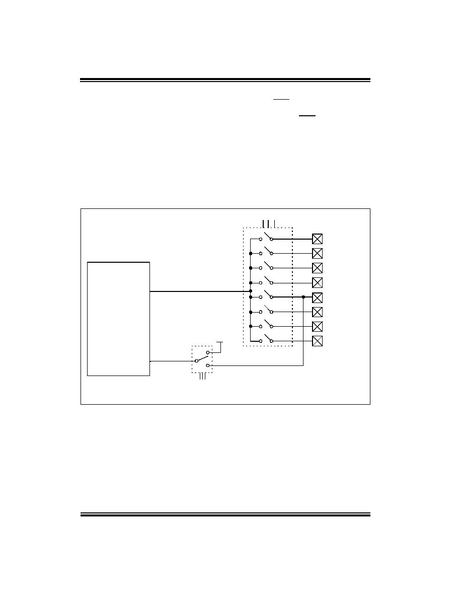
FIGURE 12-1: A/D BLOCK DIAGRAM
(Input voltage)
VIN
VREF
(Reference
voltage)
VDD
PCFG<2:0>
CHS<2:0>
000
or
010
or
100
or
001
or
011
or
101
RE2/AN7(1)
RE1/AN6(1)
RE0/AN5(1)
RA5/AN4
RA3/AN3/VREF
RA2/AN2
RA1/AN1
RA0/AN0
111
110
101
100
011
010
001
000
A/D
Converter
Note 1: Not available on PIC16C745.
11x
745cov.book Page 94 Wednesday, August 2, 2000 8:24 AM
发布紧急采购,3分钟左右您将得到回复。
相关PDF资料
PIC18C442T-E/L
IC MCU OTP 8KX16 A/D 44PLCC
PIC16C621A-40/SS
IC MCU OTP 1KX14 COMP 20SSOP
PIC16C622A-40/SS
IC MCU OTP 2KX14 COMP 20SSOP
PIC16CE623-30/SO
IC MCU OTP 512X14 EE COMP 18SOIC
PIC16CE624-30/SO
IC MCU OTP 1KX14 EE COMP 18SOIC
PIC16CE624-30/SS
IC MCU OTP 1KX14 EE COMP 20SSOP
PIC16CE623-30/SS
IC MCU OTP 512X14 EE COMP 20SSOP
PIC16CE624-30/P
IC MCU OTP 1KX14 EE COMP 18DIP
相关代理商/技术参数
PIC16C765T-I/PT
功能描述:8位微控制器 -MCU 14KB 256 RAM 33 I/O RoHS:否 制造商:Silicon Labs 核心:8051 处理器系列:C8051F39x 数据总线宽度:8 bit 最大时钟频率:50 MHz 程序存储器大小:16 KB 数据 RAM 大小:1 KB 片上 ADC:Yes 工作电源电压:1.8 V to 3.6 V 工作温度范围:- 40 C to + 105 C 封装 / 箱体:QFN-20 安装风格:SMD/SMT
PIC16C76T-04/SO
功能描述:8位微控制器 -MCU 14KB 368 RAM 22 I/O RoHS:否 制造商:Silicon Labs 核心:8051 处理器系列:C8051F39x 数据总线宽度:8 bit 最大时钟频率:50 MHz 程序存储器大小:16 KB 数据 RAM 大小:1 KB 片上 ADC:Yes 工作电源电压:1.8 V to 3.6 V 工作温度范围:- 40 C to + 105 C 封装 / 箱体:QFN-20 安装风格:SMD/SMT
PIC16C76T-04E/SO
功能描述:8位微控制器 -MCU 14KB 368 RAM 22 I/O RoHS:否 制造商:Silicon Labs 核心:8051 处理器系列:C8051F39x 数据总线宽度:8 bit 最大时钟频率:50 MHz 程序存储器大小:16 KB 数据 RAM 大小:1 KB 片上 ADC:Yes 工作电源电压:1.8 V to 3.6 V 工作温度范围:- 40 C to + 105 C 封装 / 箱体:QFN-20 安装风格:SMD/SMT
PIC16C76T-04I/SO
功能描述:8位微控制器 -MCU 14KB 368 RAM 22 I/O RoHS:否 制造商:Silicon Labs 核心:8051 处理器系列:C8051F39x 数据总线宽度:8 bit 最大时钟频率:50 MHz 程序存储器大小:16 KB 数据 RAM 大小:1 KB 片上 ADC:Yes 工作电源电压:1.8 V to 3.6 V 工作温度范围:- 40 C to + 105 C 封装 / 箱体:QFN-20 安装风格:SMD/SMT
PIC16C76T-10/SO
功能描述:8位微控制器 -MCU 14KB 368 RAM 22 I/O RoHS:否 制造商:Silicon Labs 核心:8051 处理器系列:C8051F39x 数据总线宽度:8 bit 最大时钟频率:50 MHz 程序存储器大小:16 KB 数据 RAM 大小:1 KB 片上 ADC:Yes 工作电源电压:1.8 V to 3.6 V 工作温度范围:- 40 C to + 105 C 封装 / 箱体:QFN-20 安装风格:SMD/SMT
PIC16C76T-10E/SO
功能描述:8位微控制器 -MCU 14KB 368 RAM 22 I/O RoHS:否 制造商:Silicon Labs 核心:8051 处理器系列:C8051F39x 数据总线宽度:8 bit 最大时钟频率:50 MHz 程序存储器大小:16 KB 数据 RAM 大小:1 KB 片上 ADC:Yes 工作电源电压:1.8 V to 3.6 V 工作温度范围:- 40 C to + 105 C 封装 / 箱体:QFN-20 安装风格:SMD/SMT
PIC16C76T-10I/SO
功能描述:8位微控制器 -MCU 14KB 368 RAM 22 I/O RoHS:否 制造商:Silicon Labs 核心:8051 处理器系列:C8051F39x 数据总线宽度:8 bit 最大时钟频率:50 MHz 程序存储器大小:16 KB 数据 RAM 大小:1 KB 片上 ADC:Yes 工作电源电压:1.8 V to 3.6 V 工作温度范围:- 40 C to + 105 C 封装 / 箱体:QFN-20 安装风格:SMD/SMT
PIC16C76T-20/SO
功能描述:8位微控制器 -MCU 14KB 368 RAM 22 I/O RoHS:否 制造商:Silicon Labs 核心:8051 处理器系列:C8051F39x 数据总线宽度:8 bit 最大时钟频率:50 MHz 程序存储器大小:16 KB 数据 RAM 大小:1 KB 片上 ADC:Yes 工作电源电压:1.8 V to 3.6 V 工作温度范围:- 40 C to + 105 C 封装 / 箱体:QFN-20 安装风格:SMD/SMT